Dye and Pull
Dye and Pull, formerly known as Dye and Pry is a simple method of evaluating the presence of cracks in the solder joints of surface mounted components, typically Ball Grid Arrays (BGAs). Contact Elmet LLC for your quote today!
Dye and pull testing
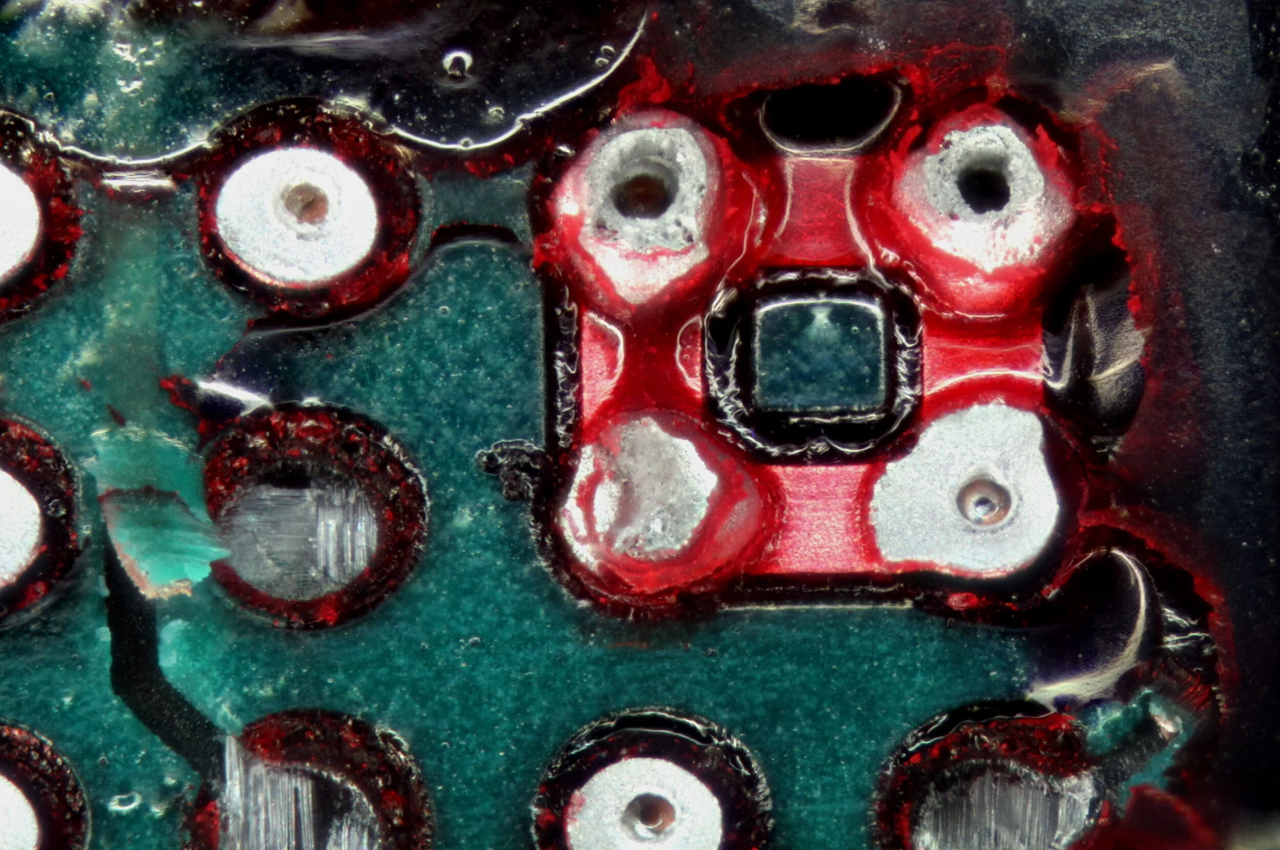
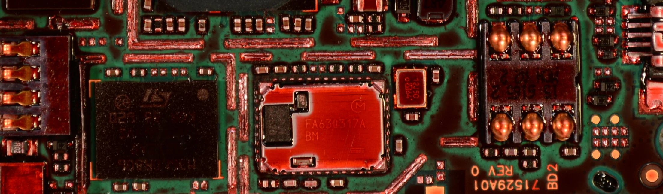
Macroscopic view of pulled solder balls.
Description of Dye and Pull Testing
The Dye and Pull Test, formerly known as Dye and Pry, is designed to detect cracks in Ball Grid Arrays (BGA), though it can be effective on other surface mounted components such as QFNs or DFNs. Detected cracks are then mapped and categorized for each component.
The method involves cleaning a circuit board or section of circuit board of solder flux and other residues before introducing a dye penetrant to the board. The dye is then allowed to fully dry before an anchor is attached to the component, which is then pulled off the board. We then inspect the surface of the circuit board and the surface of the component for evidence that the solder balls were cracked at the time they were dyed. The general method used is described in IPC-TM-650 2.4.53.
Due to the multistep sequential nature of the drying and curing process, large dye and pull requests can have longer delivery times than a standard sequential grind and polish, especially considering Elmet’s great capacity for cross-sectional throughput.
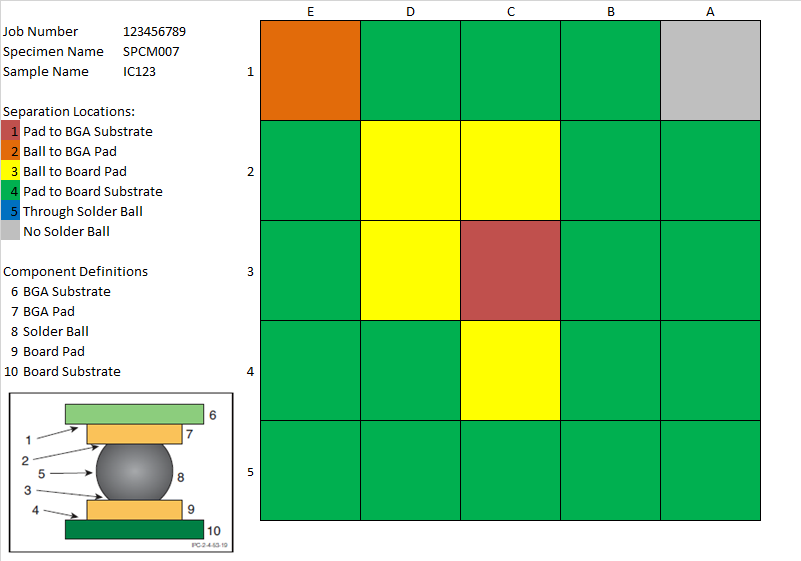
Solder Ball Separation Location Map. This map shows the solder ball separation locations of a 5x5 solder ball grid array.
Deliverables
Elmet supplies overview photographs of every dye and pull target and labeled, high magnification photographs of cracked solder balls when they are present. Categorization and mappings of all cracks are also documented for each dyed and pulled component. Additional photographs may also be delivered as agreed upon with the customer. The photographs are organized into a written report along with a summary of observations. CLICK HERE for an example report.
What to do next
In order to provide you with quality analysis and an accurate quote, we need to know certain things.
We need a layout or photograph of the circuit board with the target components marked. Most customers draw a box around each target component indicating the desired target and include a technical drawing of each type of BGA for ease in labeling, and so we know the size of the ball grid. The photograph below shows an example. Sometimes it is easier to provide us with a list of target components by their name in the layout, and we will label solder balls according to industry standards.
Layout images are typically marked with a simple box.
We also need to know how many circuit boards you want evaluated, and we need to know if they are all arriving simultaneously or if some will arrive this month and more next month.
We need a specific scope of work. This could be simple, such as “inspect for cracks,” or it can be more detailed, such as “inspect the board per ICP-A-610, followed by dye and pull and crack inspection.”
Call or email us with any questions that you have about the process, our capabilities, delivery, or price. Alternativley, you can submit the layout and scope of work, and we’ll get back to you with a quote. Or, visit our Price Estimation form if you want a fast, informal idea as to scope of your project!