X-Ray Services
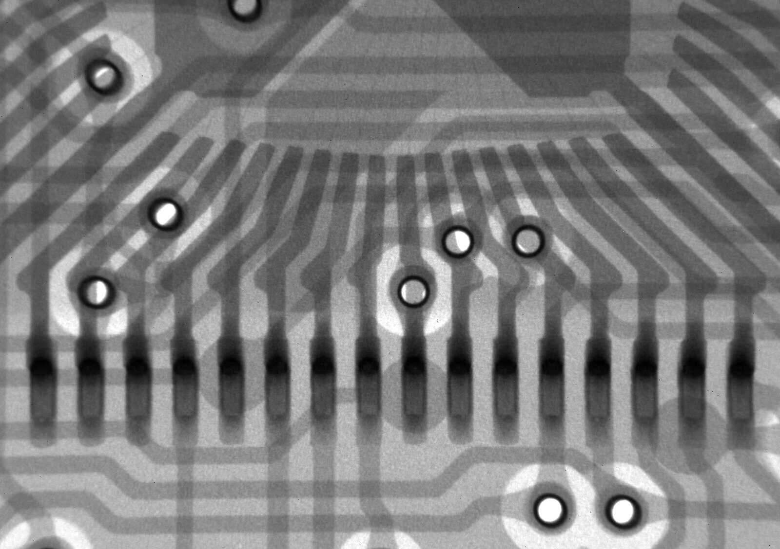
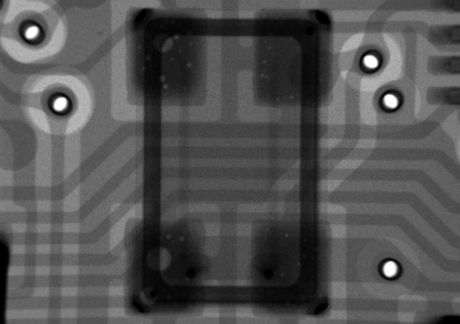
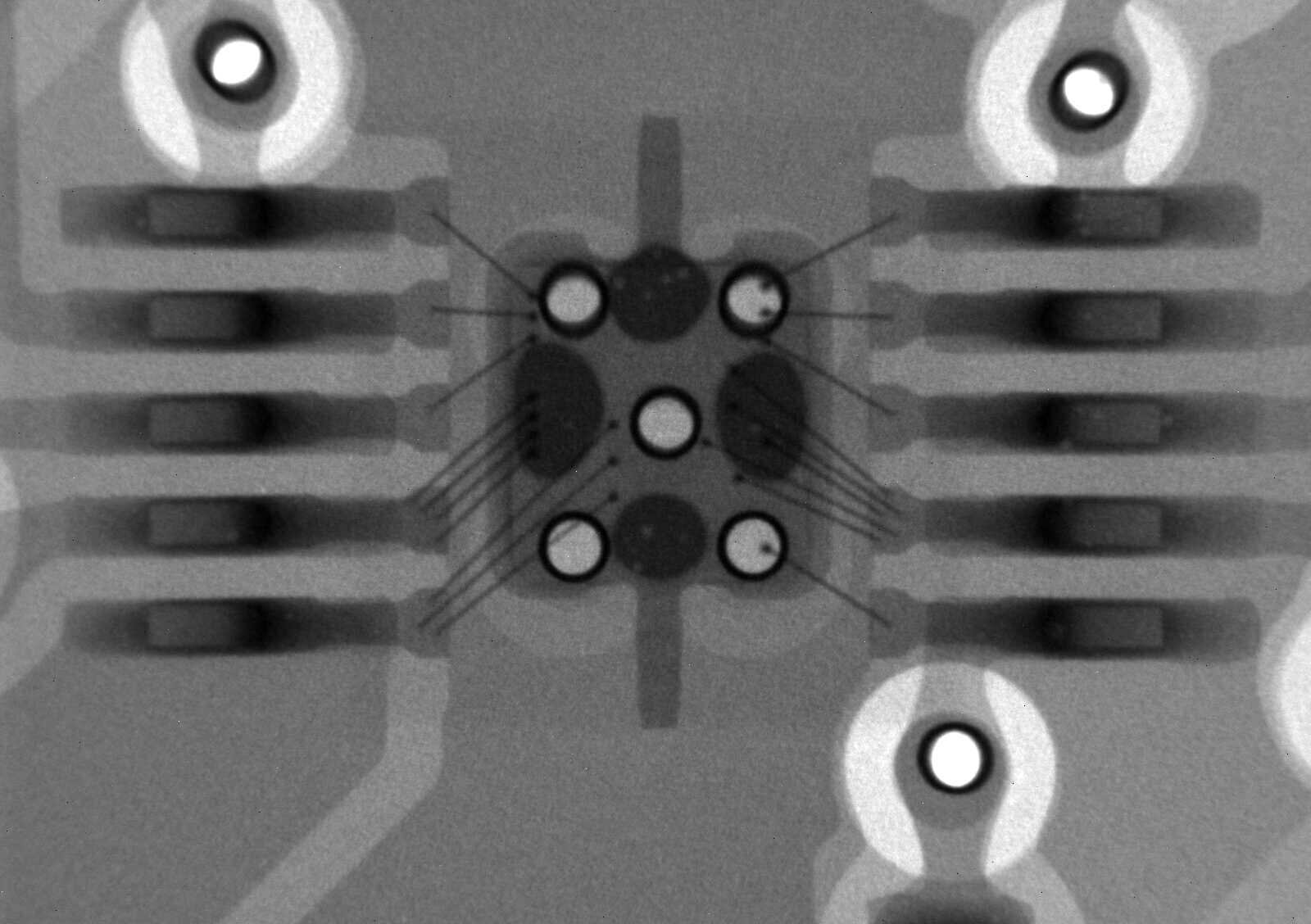
Our Phoenix Nanomex X-ray machine is designed for high resolution imaging of PCBs, PTH, solder joints, and components. With the ability to see features as small as 1 micrometer in width, we can look for solder defects, solder voids, displacements, and cracks.
X-ray services
Our Phoenix Nanomex X-ray machine is designed for high resolution imaging of PCBs, PTH, solder joints, and components. With the ability to see features as small as 1 micrometer in width, we can look for solder defects, solder voids, displacements, and cracks. We can also use X-ray to determine the location of an internal feature prior to cross sectioning.
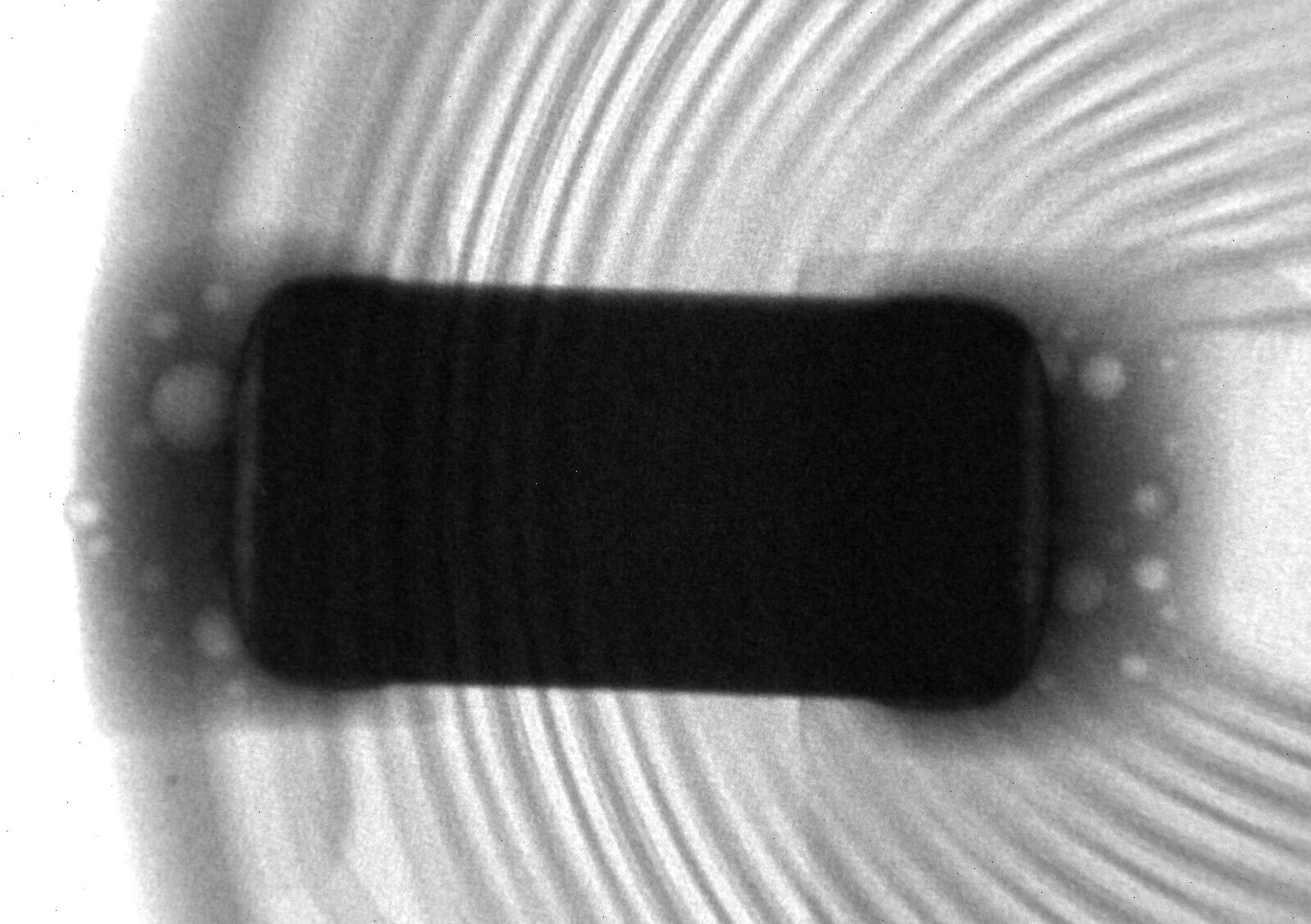
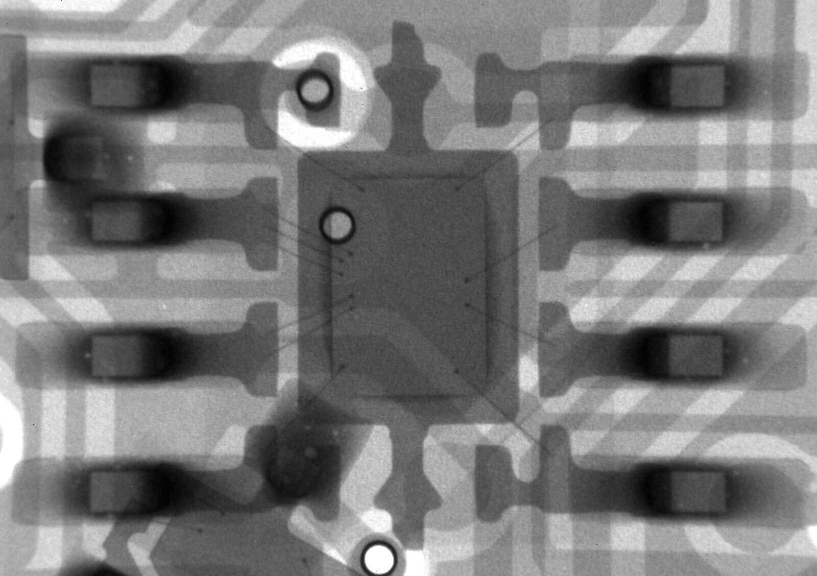
Capacitors overlap on opposite sides of the PCB
This X-ray image shows an SMT capacitor on the top side of the PCB and an electrolytic capacitor on the bottom side of the PCB. Despite the overlap the solder voids are visible.
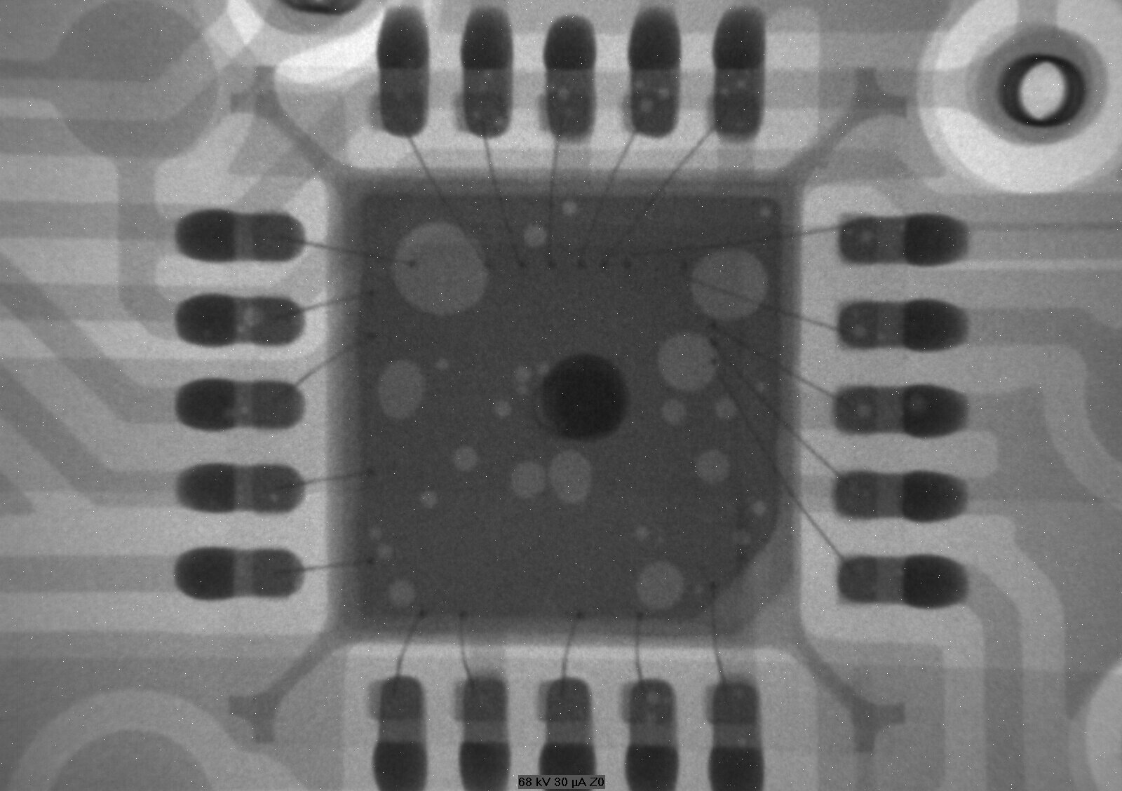
Detection of solder voids is one of the most common uses of X-rays in PCBA inspection. Voids are almost always present in solder joints; they appear as lighter colored areas within the darker solder.
Elmet uses software to detect and outline the void areas within a solder joint. The image below shows an X-ray image with void areas outlined with yellow. The void fraction is calculated as the area of void divided by the area of the solder joint in accordance with JEDEC standard JESD217.01.
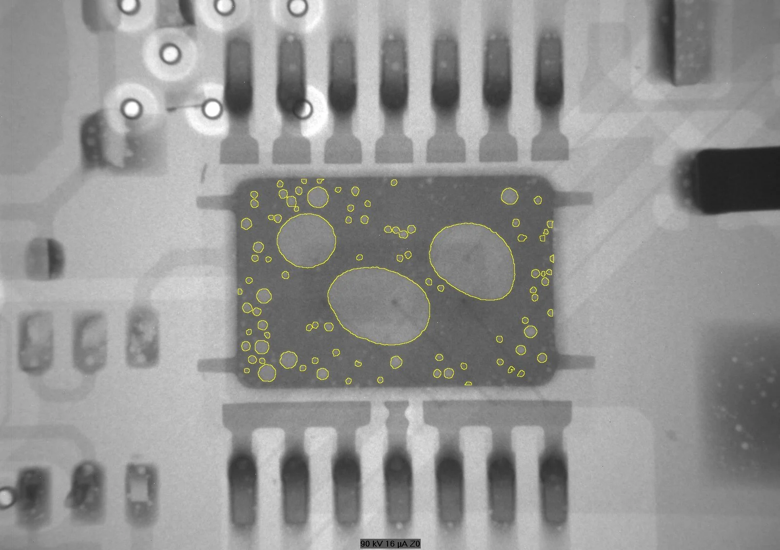
Void fraction measurement by X-ray
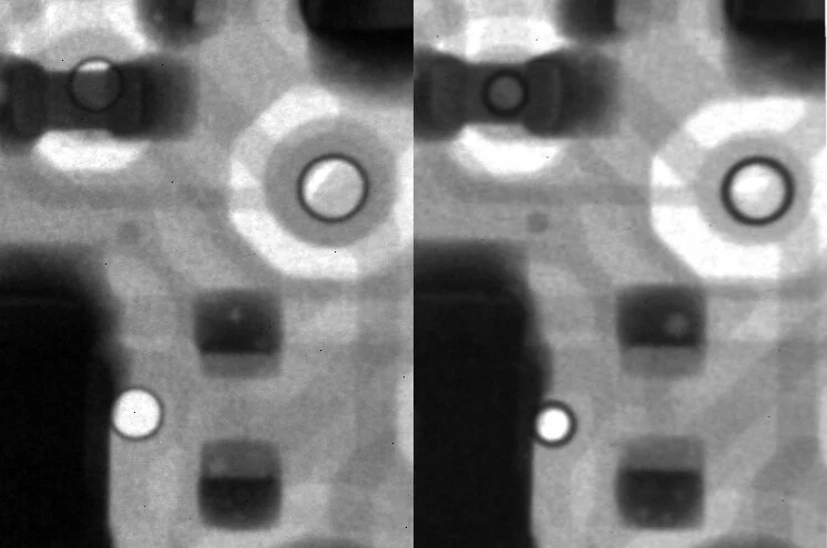
X-ray imaging can detect cracks in solder joints, copper traces, internal layers, and PTH when the plane of the crack is parallel to the X-ray beam. The X-rays pass unimpeded through the crack and the crack appears as a bright line in the X-ray image. Because of the specific orientation required for crack detection by X-ray, cross sectioning can by a better way to detect cracks in solder joints. Copper traces are good candidates for X-ray crack detection because the cracks in copper traces are usually oriented correctly for X-ray detection.
We also use X-ray as a diagnostic tool. Sometimes a customer has no good lead on the cause of circuit failure. X-ray examination can produce clues that are completely unexpected. We have detected changes in via diameter or fill, land size, and trace location even though the PCB supplier said “no change was made”. These types of exploratory examinations can produce surprising revelations, or verify that no physical problems or changes are evident.
Call or email us with your X-ray requirements. CLICK HERE for an example report.