Cross-Sectional Analysis
Cross sectioning is also known as dissection, metallographic preparation, and micro sectioning. Cross sectioning of circuit boards is done in support of several types of evaluations, including crack detection, IPC-A-6012 inspections, plate thickness measurement, and failure analysis.
Cross Sectional Analysis
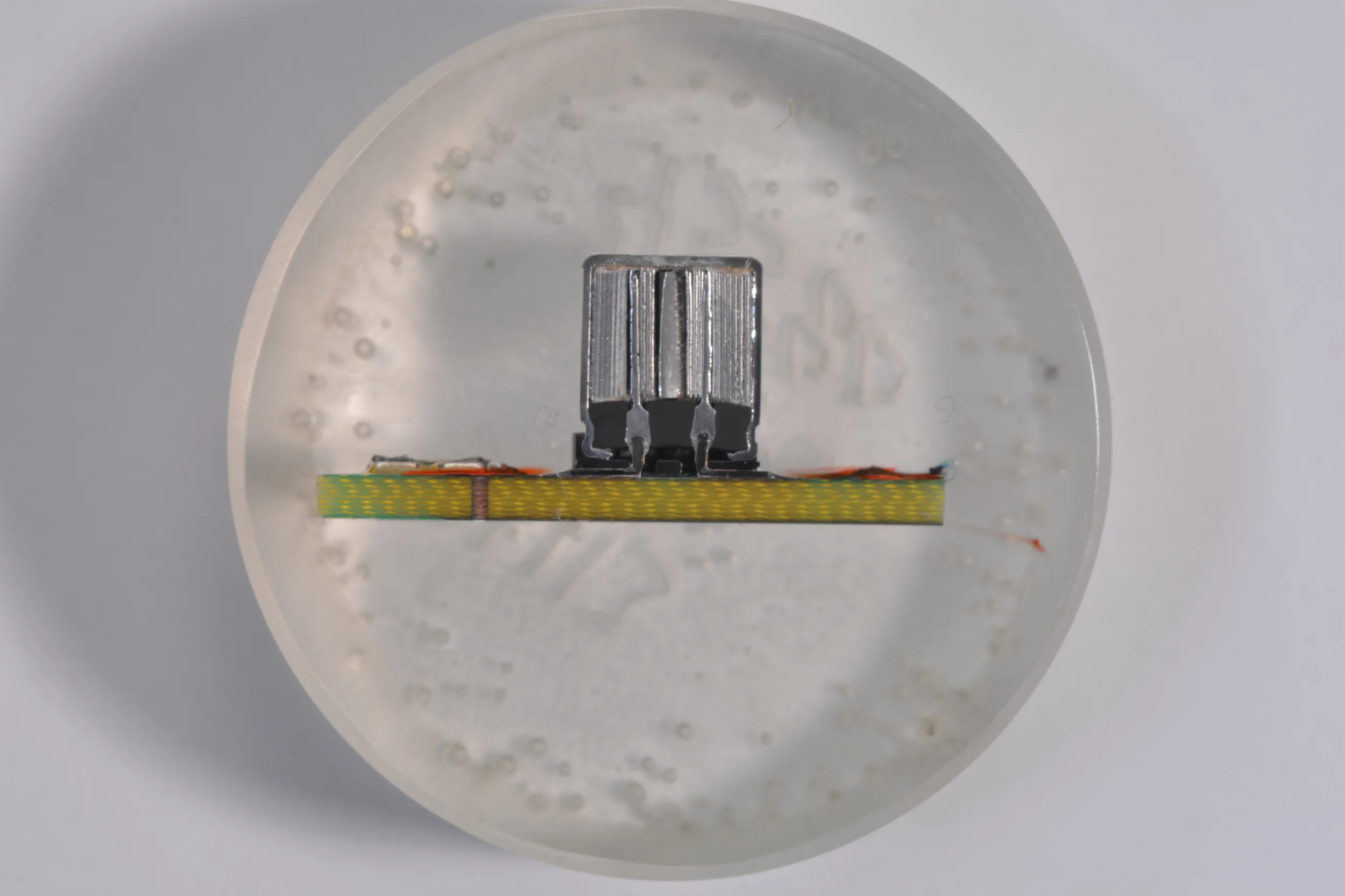
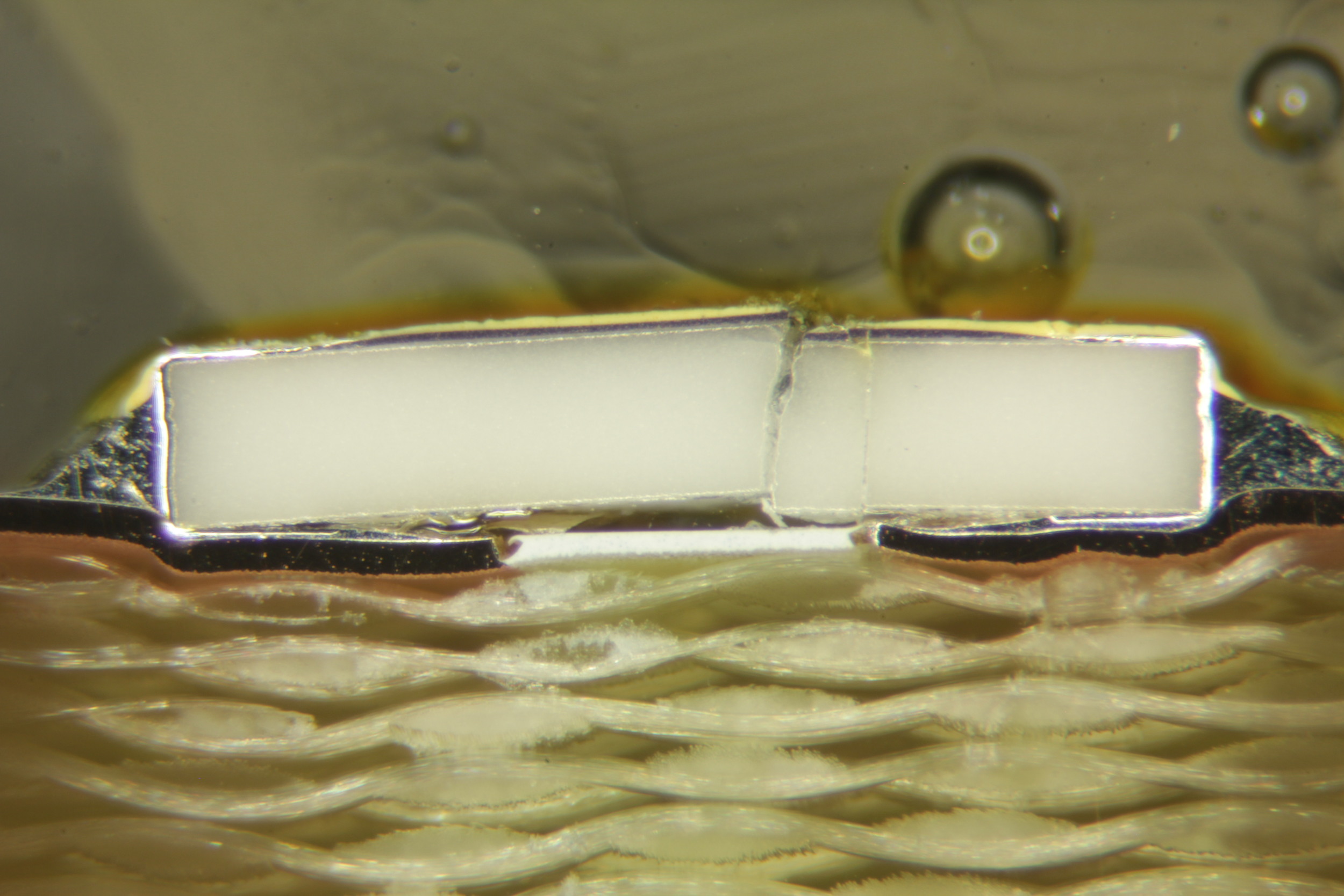
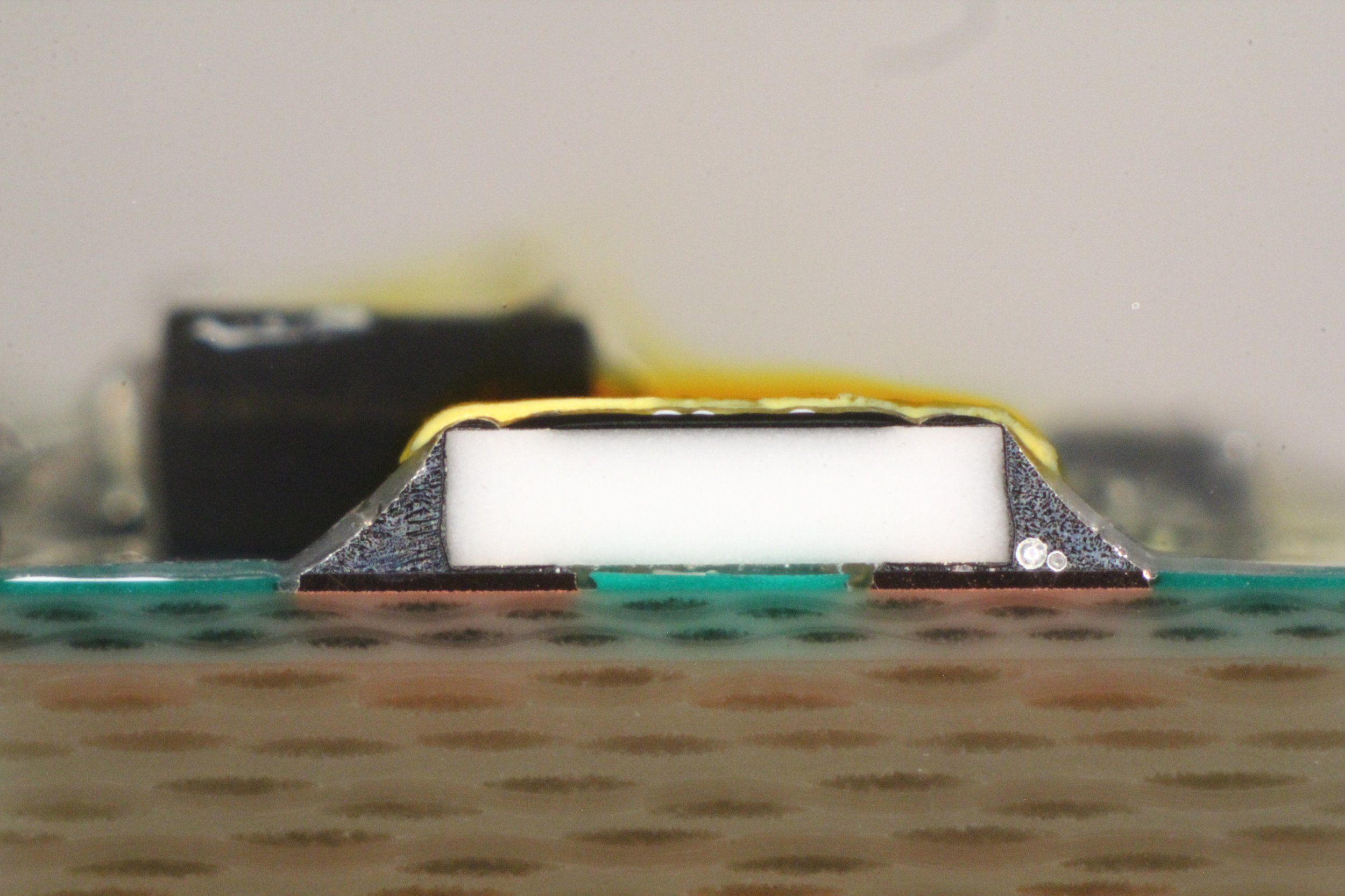
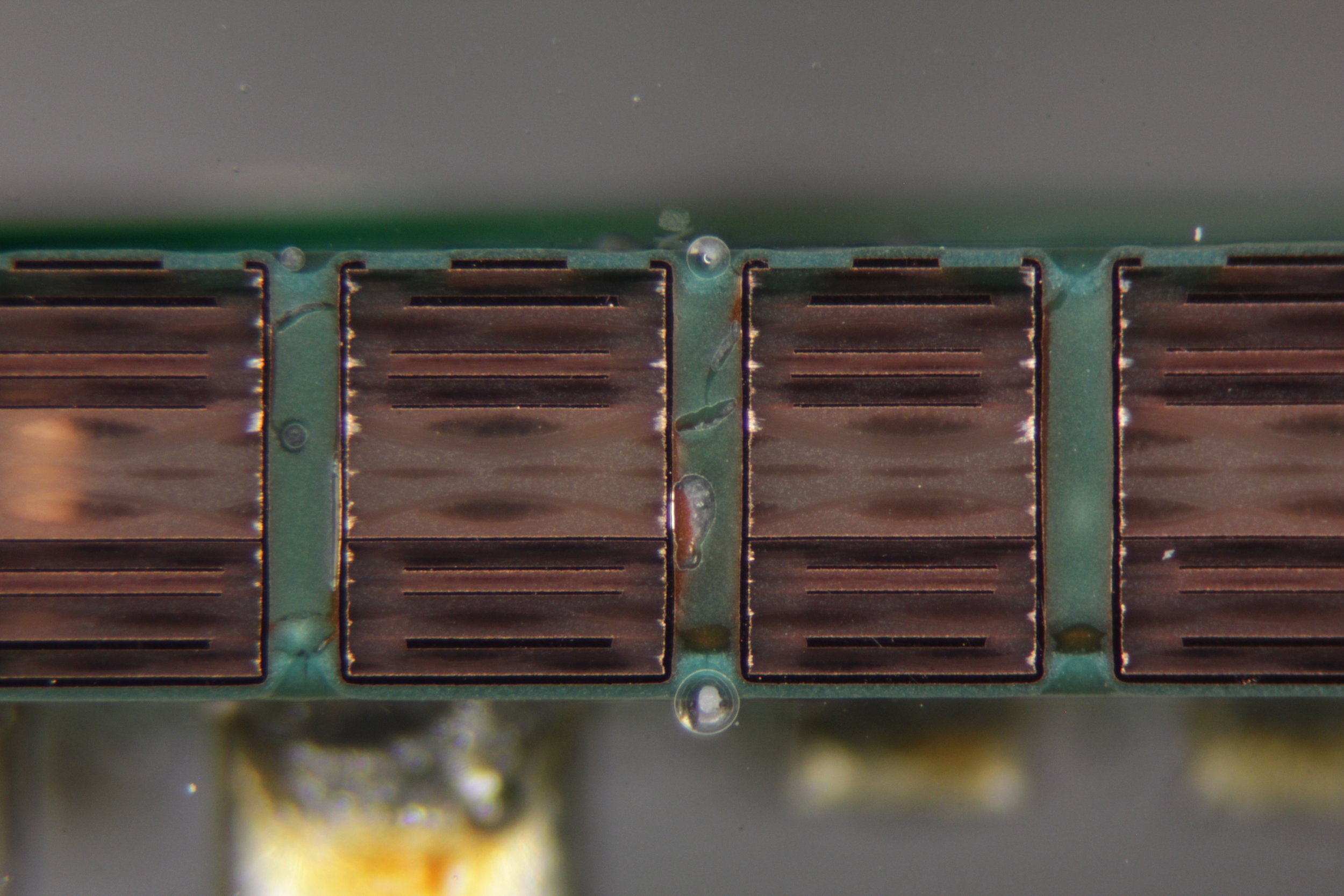
Capacitor cross-section
Cross sectioning is also known as dissection and micro sectioning. It entails cutting a circuit board to retrieve an area of interest, potting the targeted item in epoxy, and grinding/polishing to a particular plane in order to see internal features of the circuit board, solder joint, or component.
Cross sectioning is done as part of component replacement studies, problem diagnostics, field failure studies, product characterization, production issue studies, solder joint crack detection, void measurement, via examination, plate thickness measurement, and PCB evaluation. For example, automotive companies require DV and PV thermal cycle testing that tends to create fatigue cracks in solder joints; cross sectioning is performed to identify and measure those cracks.
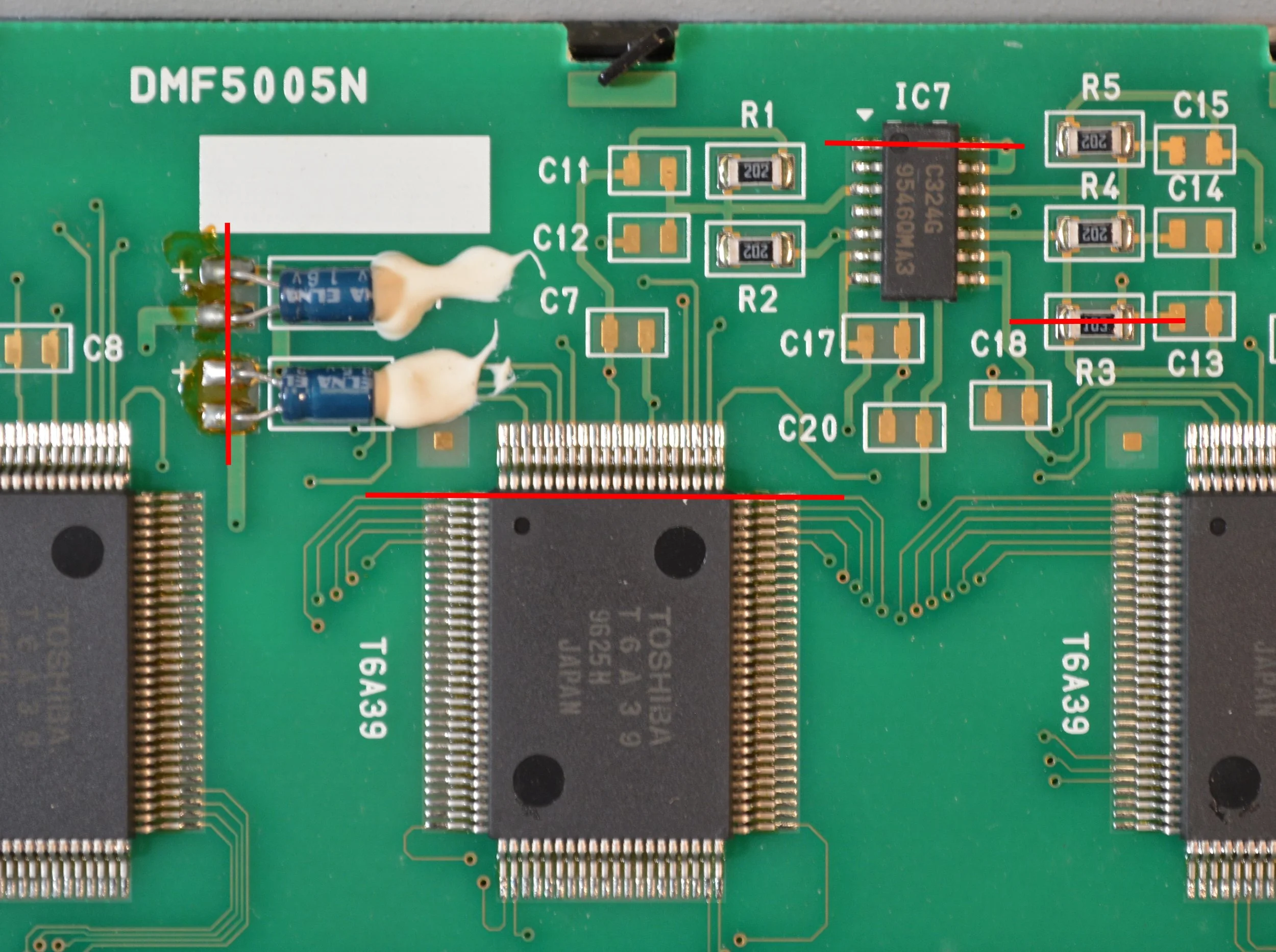
Customer supplied image showing the targeted cross section locations.
Description of Cross-Section Analysis
The technical procedure for cross sectioning is given in ICP-TM-650 2.1.1, but the evaluation begins further upstream when our customer selects several, or many, items on the PCBA that they feel should be evaluated. The selection is based on the soldering process used, the size of the component, the location on the PCBA, and their experience with the PCBA. At least one component representing each type of solder joint is selected, including discrete SMT resistors or capacitors, BGAs, QFNs, vias, through-board mounted components, etc. The selected components are called targets, and the intended cross section plane through a target component is called the target plane. The target plane traverses a particular row of the BGA, or a pair of QFN terminals, or the center of a discrete component.

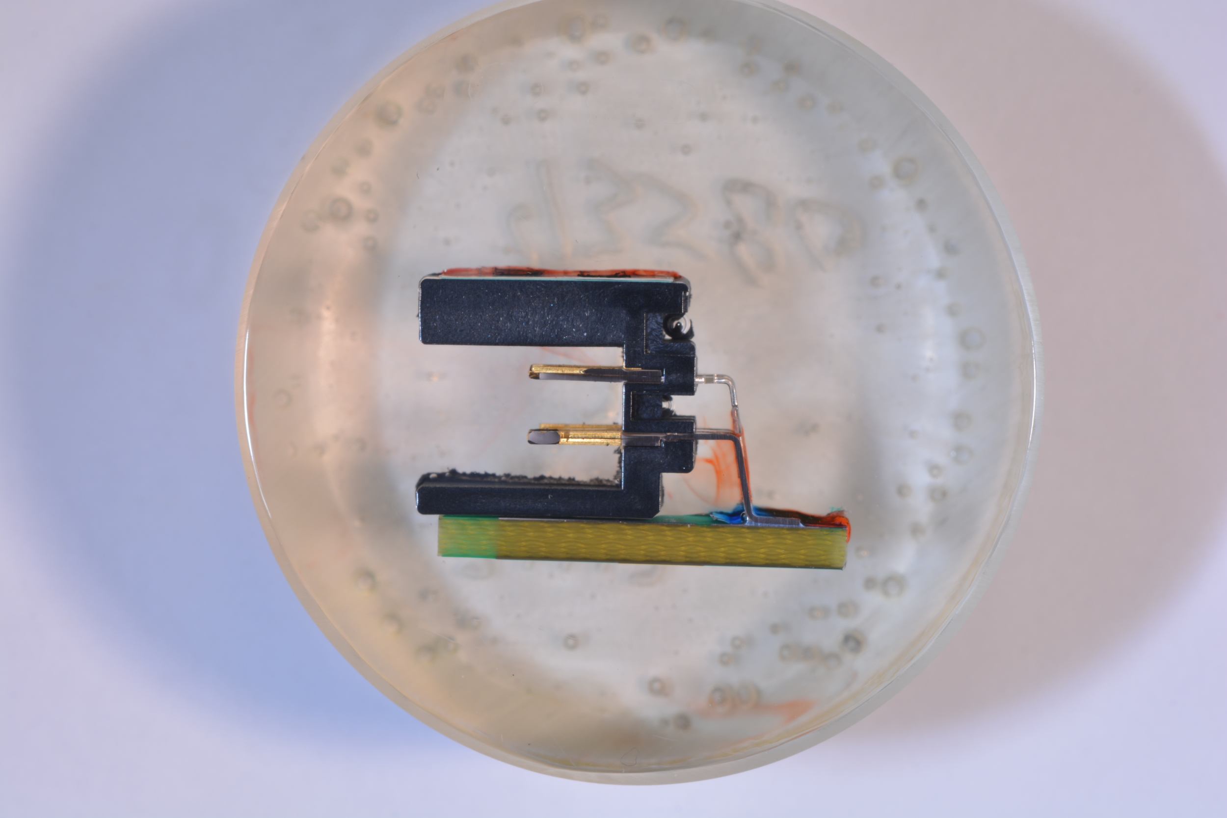
Round mounts are most common, but Elmet makes square mounts to polish multiple perpendicular planes.
The circuit board must be cut with a diamond saw to separate target components prior to potting and polishing. The saw cut is always made outside, never through, the target component. The target component is placed in a small cup (25mm, 30mm, 40mm and 50mm diameter cups are common sizes) which is then backfilled with epoxy under vacuum to create a “mount”, or as it is sometimes called, a “puck”. The hardened epoxy stabilizes the target component for handling and grinding. The mount is ground nearly to the target plane using successively finer grits of silicon carbide grinding papers, and then may be fine-ground using diamond on a cloth.

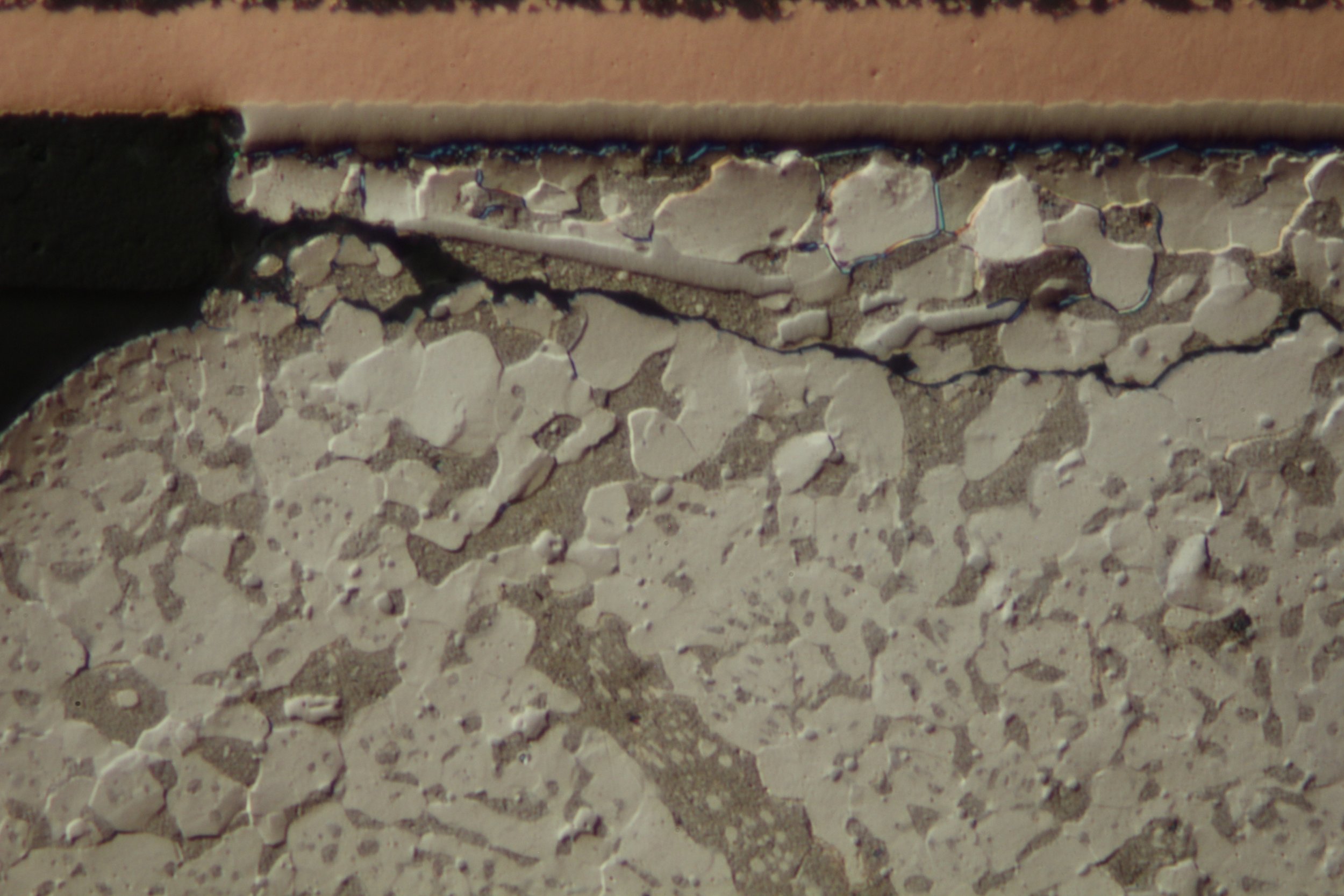
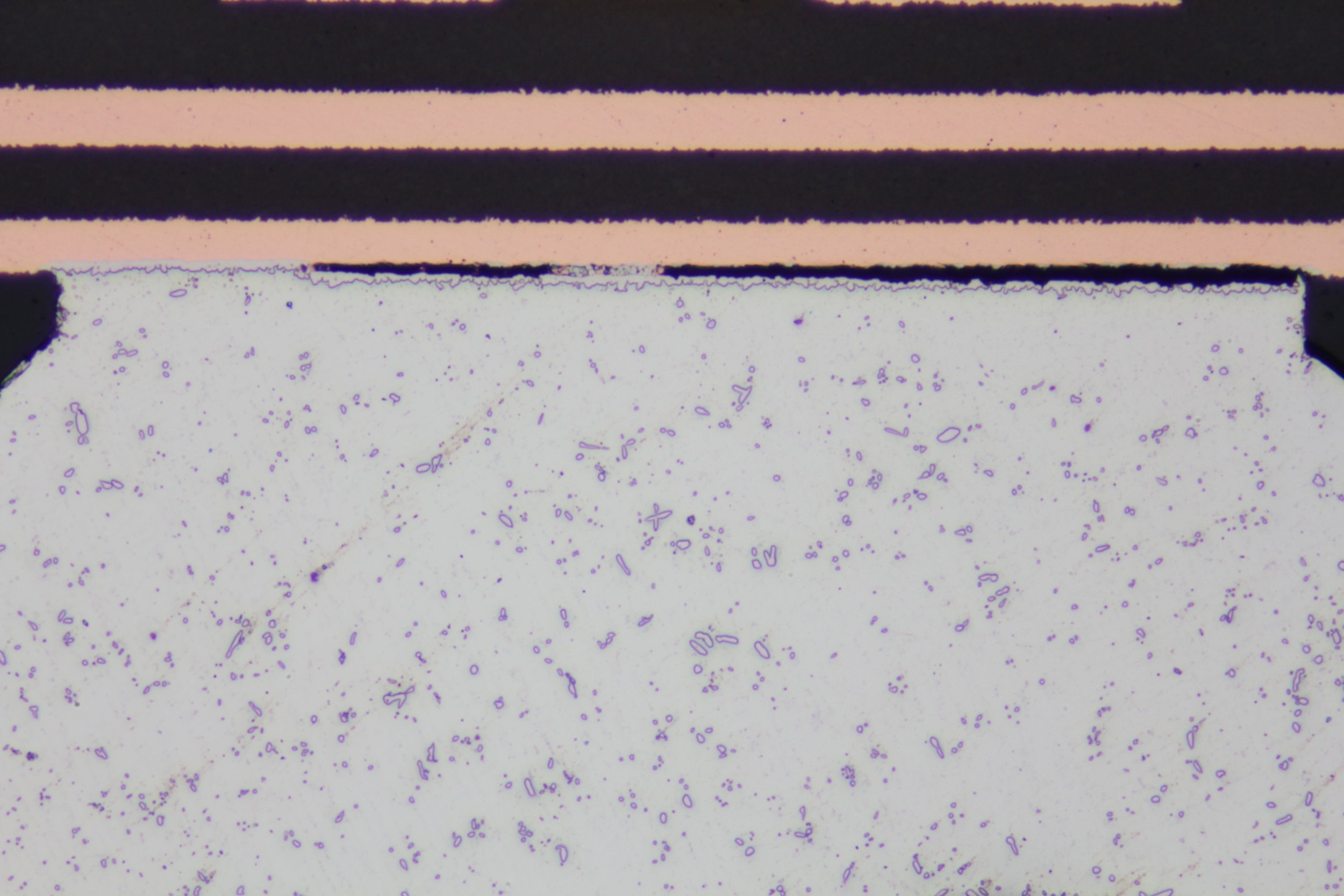
Etched microsection of a copper plated through hole.
Procedures at this stage vary with the laboratory and the component being cross sectioned, but generally the mount is processed through successively finer grits of diamond, alumina, and/or silica abrasive. The use of finer and finer abrasive assures there is no smearing or scratches remaining on the polished surface, and no material damage below the surface. At this point the polished target plane can be etched, if desired, to reveal metallurgical features prior to inspecting the cross section using optical or electron microscopes.

Elmet’s polishing facilities.
THroughput
Elmet has 5 grinding and polishing systems capable of being programmed for grinding and polishing force, speed, and time, with automated dispensing of abrasive grit and lubricant. This allows us to separate grinding and polishing steps onto separate equipment, avoiding cross contamination and reducing the manpower needed to process a sample. As a result, Elmet’s capacity approaches 100 samples daily with generally shorter turn-around time and better quality than other labs.
Accuracy
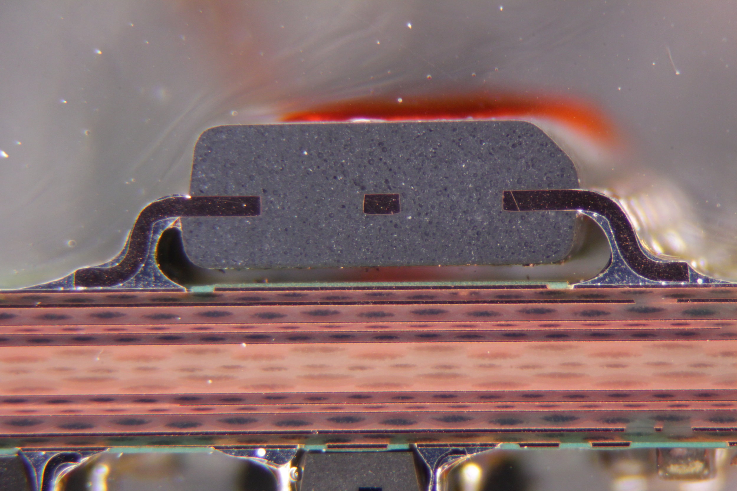
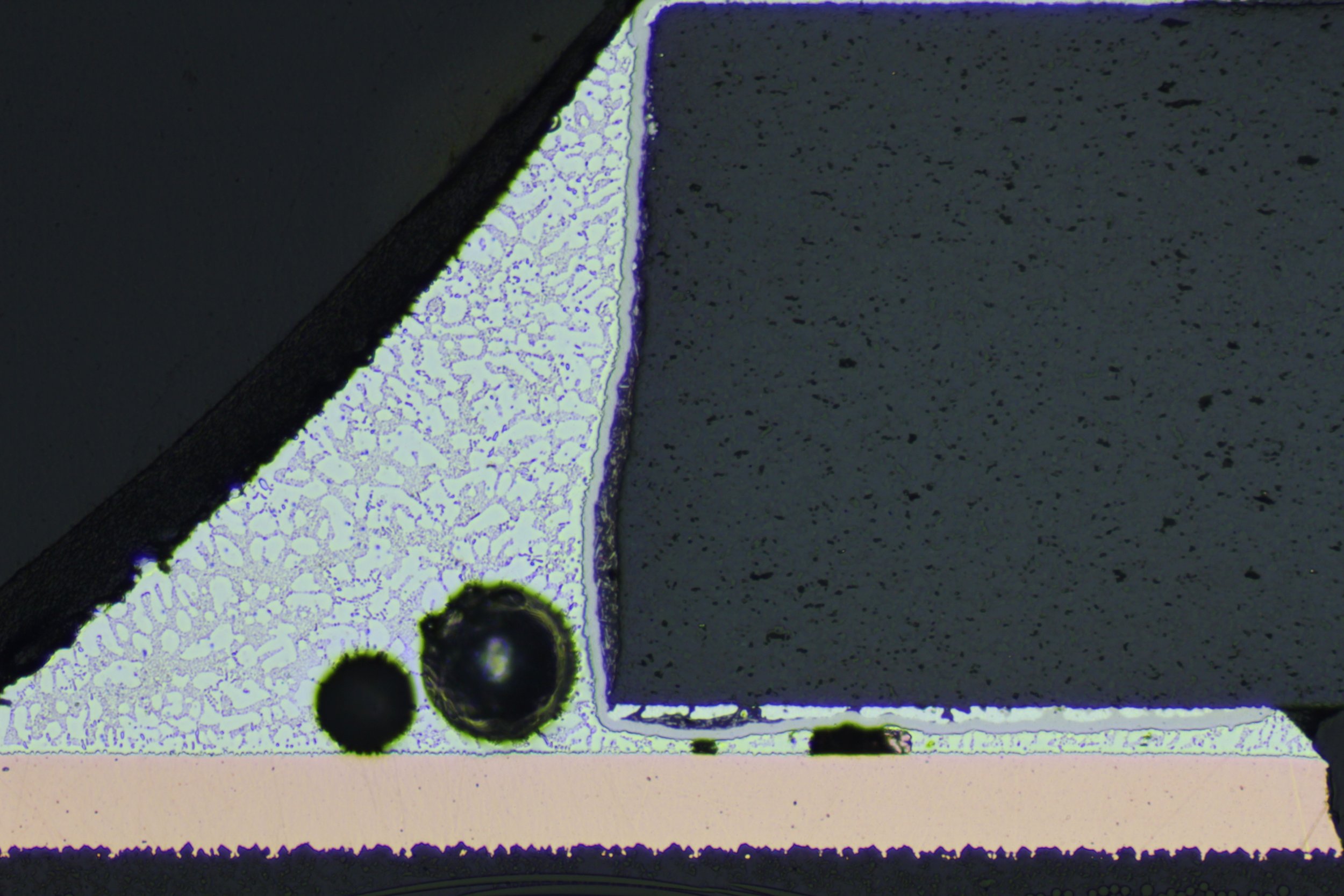
In many cases the accuracy of a target plane is not especially important; the middle third of a ceramic capacitor is near enough to the center and may be acceptable. Other applications require more accuracy. For instance, in order to accurately measure the plating thickness of a plated through hole the cross section needs to go through the center. IPC’s technical procedure for polishing, ICP-TM-650 2.1.1, allows for a tolerance of 10% of the hole diameter. Elmet can easily meet this standard and regularly holds to much tighter tolerances. The gold wire bond inside an IC in the image at the right is approximately 50 microns in diameter, for example. Some of our customers have requested precise cross-sectioning to take physical measurements of very small and inaccesible components, stand off distances, or angle measurements on circuit boards, automotive components, medical devices and RF equipment.

Elmet won an award for this optical photomicrograph showing a cracked solder ball. This image was acquired using differential interference contrast.

Evaluation
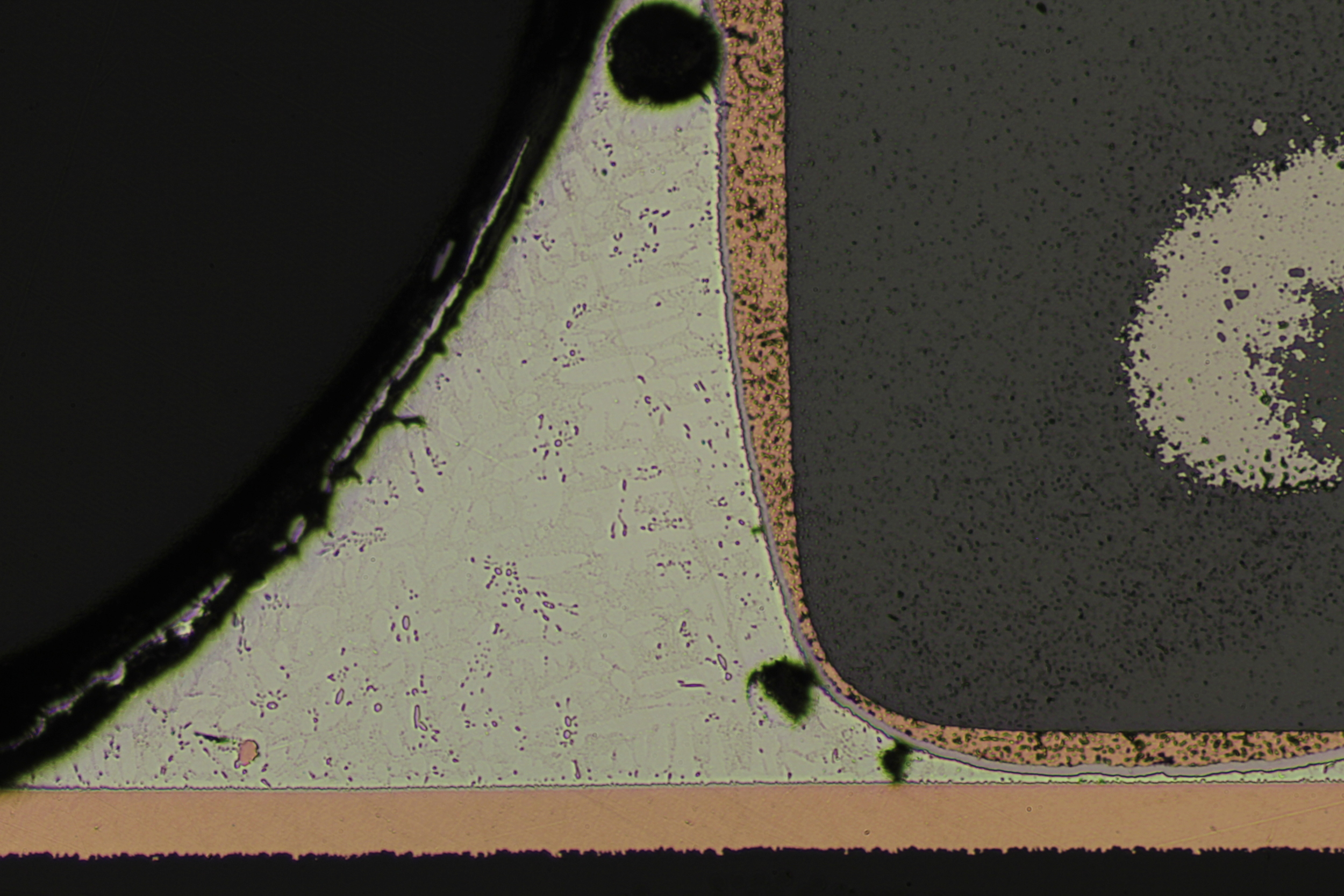
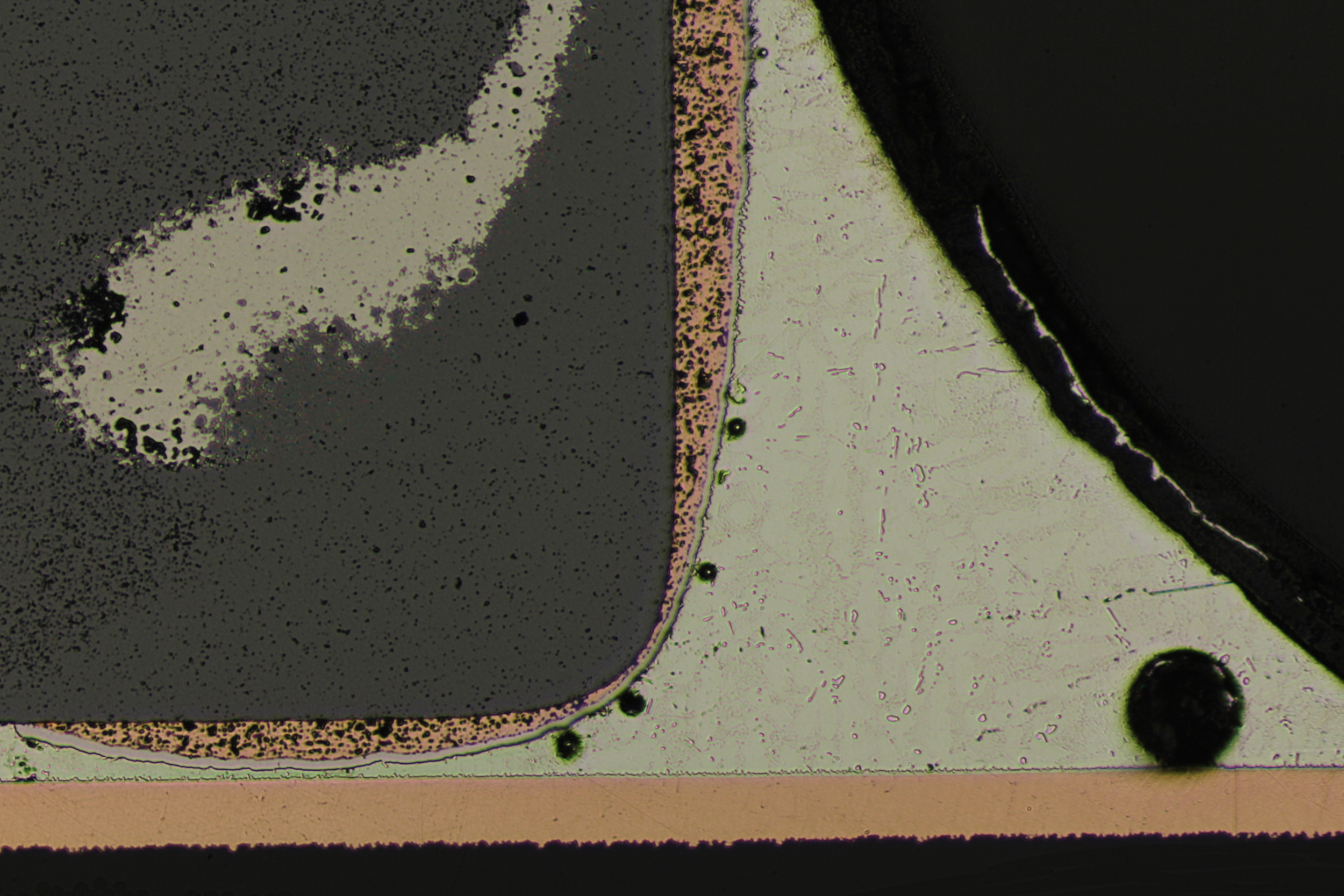
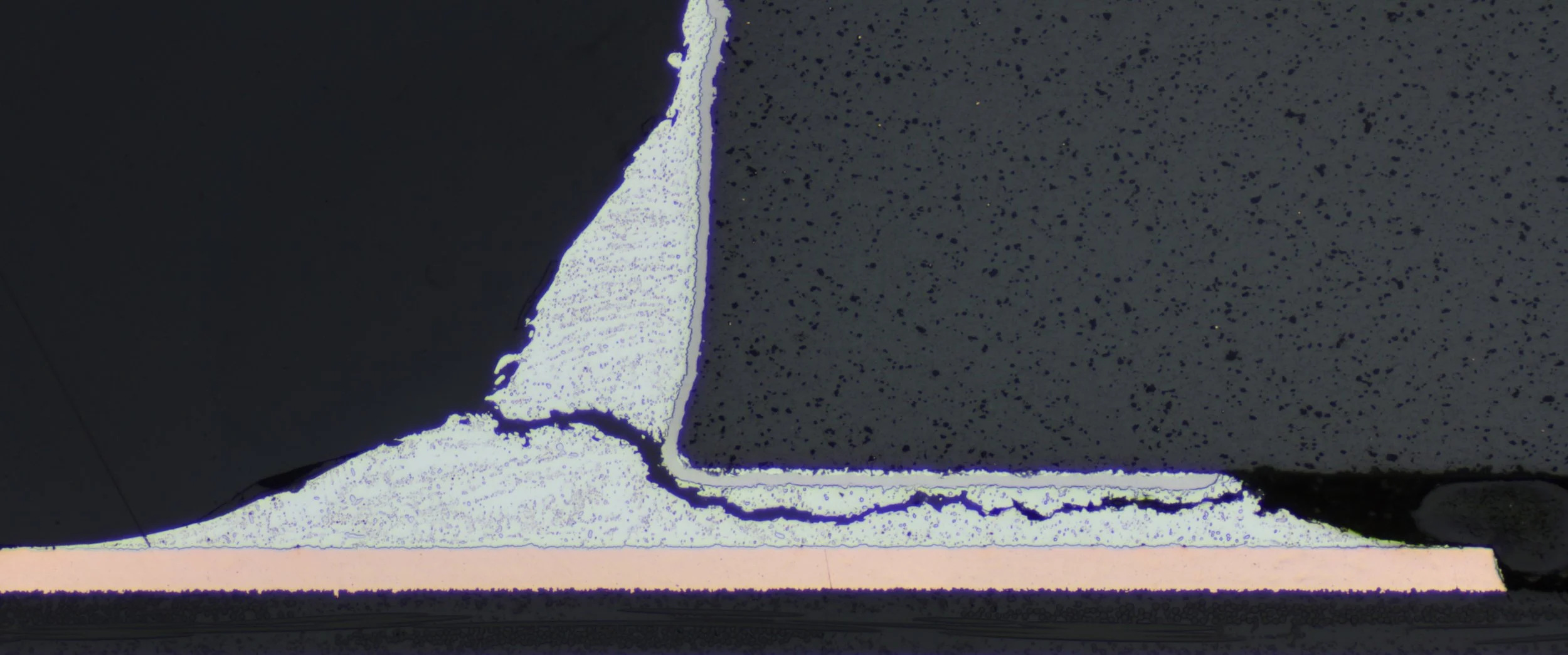
Elmet evaluates the polished cross section using optical and/or electron microscopes. Solder joints are inspected for cracks, voids, intermetallic compound (IMC) layer thickness and other features of interest. Cracks and large voids are measured and reported. PTH are evaluated for nodules, voids, solder fill, cracks, plating thickness, nail-heading, etc. PCBs can be evaluated for delamination, voiding, layer thickness, and other PCB problems.
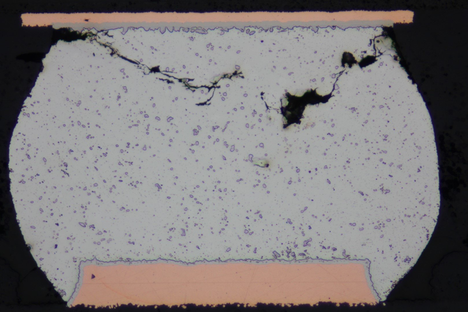
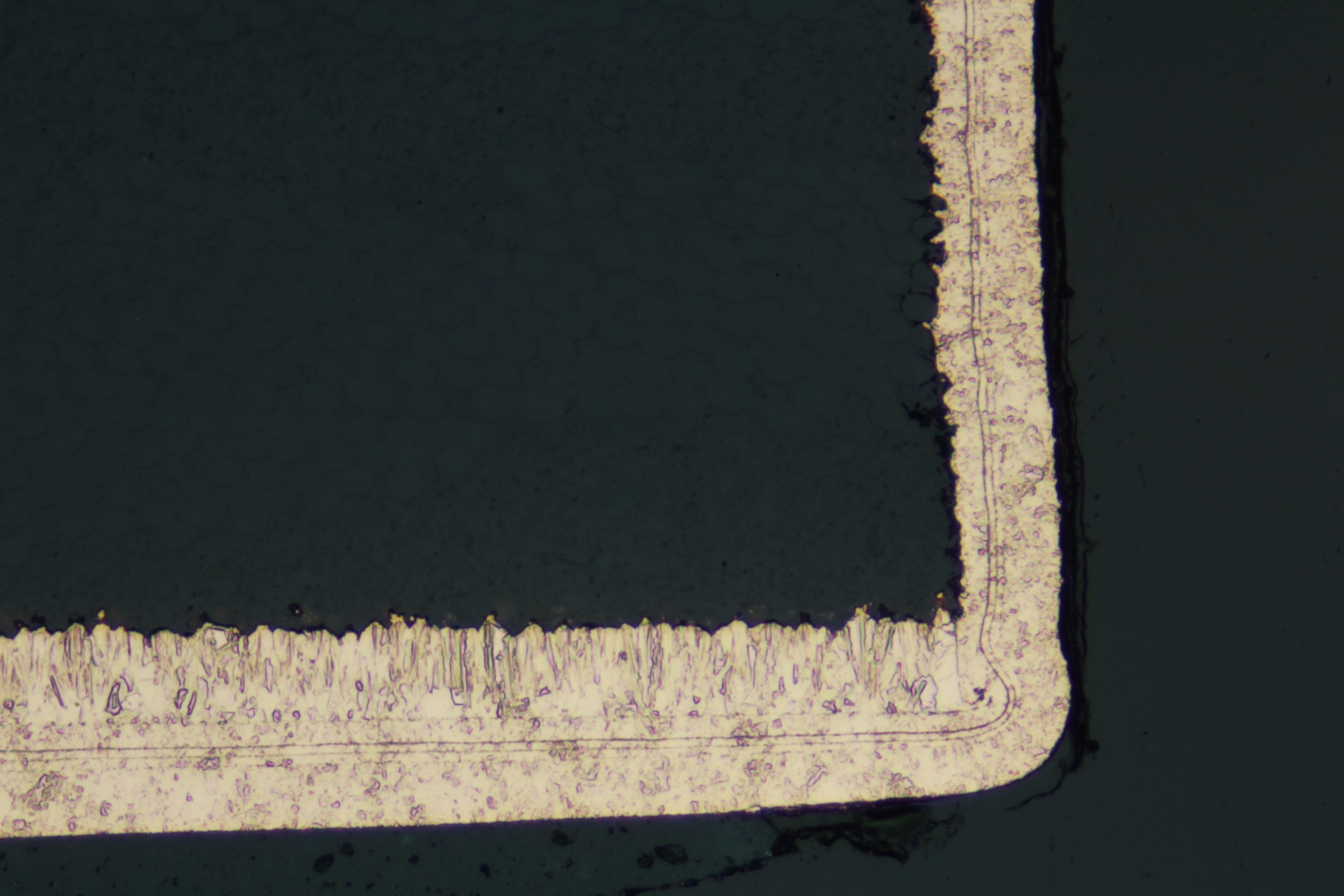
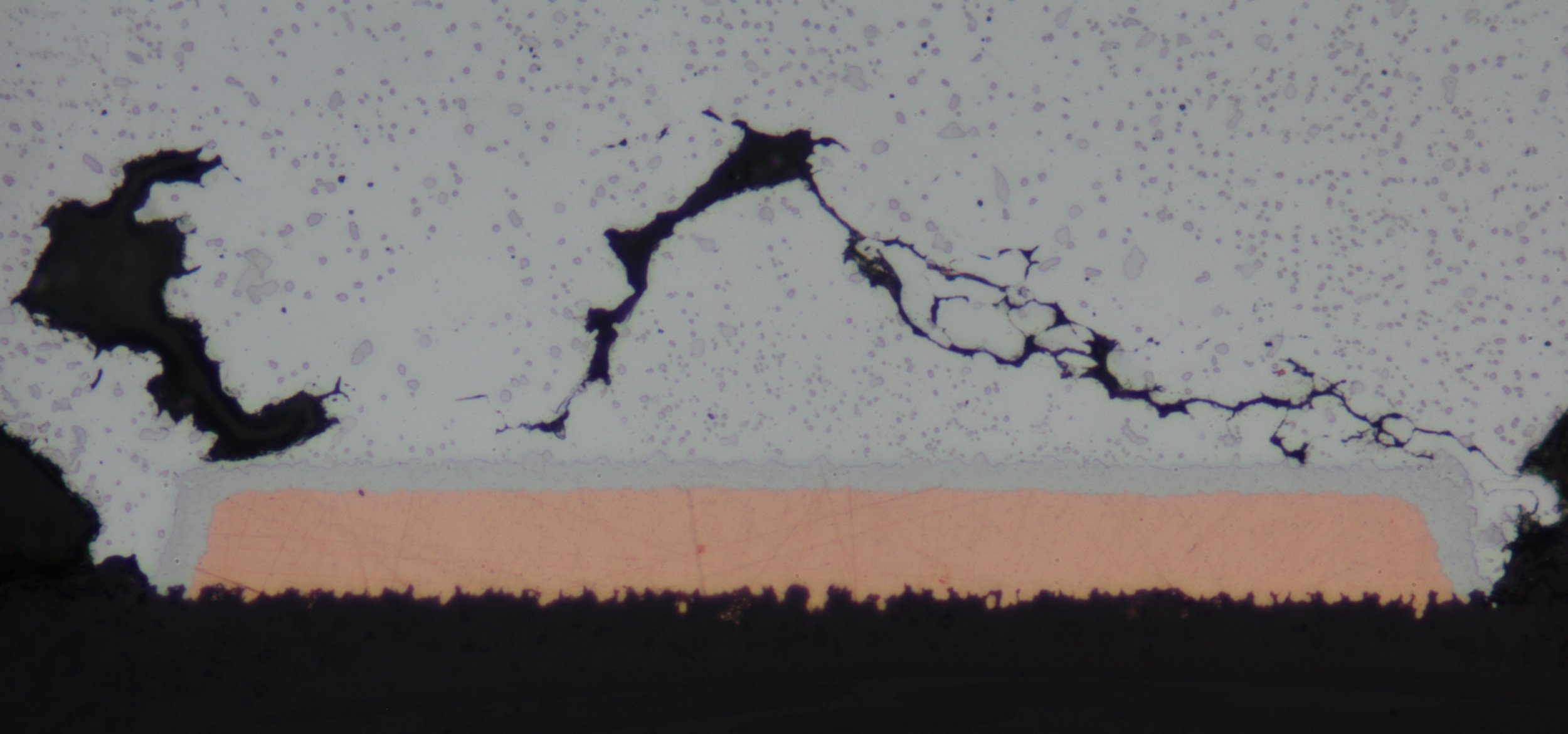
SMT resistor solder crack.

Image of a cracked solder ball acquired using cross polarized light.
When examinations are conducted with a scanning electron microscope we use secondary electron imaging, backscattered electron imaging, or energy dispersive spectroscopy to provide an elemental analysis.
When examining cross sections with an optical microscope Elmet uses bright field, dark field, cross polarization, and differential interference contrast imaging to reveal features of interest. We have won several awards for our photographs. The Gallery page of this website contains many photographs that represent our typical product.
Deliverables
Elmet provides a written report containing a summary of all observations and measurements. We provide overview and high magnification photographs of every cross section, and we photograph all cracks and other feature of interest. We measure crack length as a percentage of the solder joint length, and void area as a percentage of solder joint area. And, we identify the IC terminals or the row and column of the BGA solder balls on the overview photographs. CLICK HERE for a sanitized example report.
Specifications and standards
Evaluation is directed by customer specifications, and we work with all the major automotive specifications including GMW3172, Ford CETP E-412, Toyota TSC0509, Stelantis CS.00056, as well as industry standards such as J-STD-001, IPC-A-600, IPC-6012, IPC-6018, JESD22-A121 and others.
Call or email us with any questions that you have about the process, our capabilities, delivery, or price. Or, you can email us the layout and scope of work and we’ll get back to you with a full quote. Or, visit our Price Estimation form if you want a fast, informal idea as to scope of your project!
See additional photos below